

Models
-
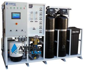
AP10K-LX
Industrial Reverse Osmosis
The AMPAC USA Industrial Reverse Osmosis 10,000 GPD system, Model AP10K-LX, delivers consistent, high-quality pure water for commercial and industrial applications.
10,000 GPD 1.6 m³/hr
View specifications -
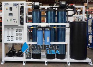
APRO-DI15
APRO-DI15 High Purity Water Treatment & Lab Pure Water System
Ampac USA's Pre-Engineered Laboratory Water Systems are designed to serve as the centralized, purified water source for a variety of academic, medical, and other research laboratory facilities.
View specifications
Need an output between two models, or a different feed water? Send us your numbers
About Semi-Conductors
Sizing a system? Send your flow rate and a feed-water analysis, and an AMPAC engineer will work out the configuration with you.
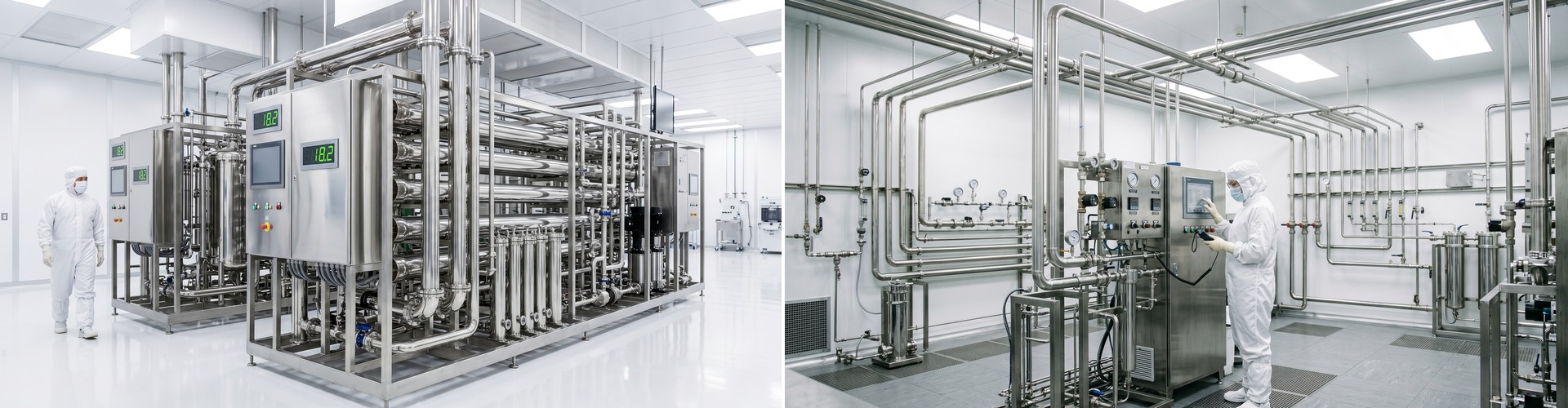
Semiconductor fabrication uses ultrapure water as both a process chemical and a cleaning agent at nearly every step - wafer washing, photolithography, chemical mechanical planarization, and final rinse before packaging. Any ionic contamination in the rinse water deposits on the wafer surface and affects electrical performance. The industry standard for process water is Type E-1 ultrapure water with resistivity at or above 18.2 megohm-cm and particle counts below 1 per milliliter at 0.05 microns.
Getting there requires a multi-stage treatment process. Municipal or well water enters the system and goes through softening or antiscalant pretreatment, followed by activated carbon filtration to remove chlorine and organic compounds that would foul downstream membranes. Two-pass reverse osmosis then removes over 99.9% of dissolved ions. Electrodeionization (EDI) or mixed-bed deionization polishing follows the RO stage, bringing resistivity to the 18.2 megohm-cm specification. Final filtration through sub-micron cartridge and ultrafiltration membranes removes particles and trace organics before delivery to the fab floor.
AMPAC USA designs and manufactures ultrapure water systems for semiconductor and electronics manufacturing. Systems are engineered to the specific flow rate, water quality target, and facility footprint of each installation. For existing fabs expanding capacity or upgrading aging UPW infrastructure, AMPAC can work within the existing utility routing and building constraints. For greenfield builds, AMPAC provides system design documentation suited for permitting and facility engineering review.
Resistivity monitoring at multiple points in the system is standard on AMPAC UPW skids. Real-time monitoring detects resin exhaustion, membrane performance degradation, or upstream upset conditions before they affect process water quality. Remote monitoring capability allows quality data review without continuous on-site operator attention.
AMPAC maintains a global service network and supplies replacement membranes, resin, and cartridge elements to ensure process continuity for operating systems. Contact AMPAC USA at (909) 548-4900 to discuss ultrapure water system requirements for your facility.
Frequently Asked Questions
What resistivity level is required for ultrapure water used in semiconductor fabrication?
Semiconductor wafer processing requires ultrapure water at 18.2 megohm-cm resistivity, the theoretical maximum for pure water at 25 degrees C, along with TOC below 1 ppb, dissolved oxygen below 1 ppb, and particle counts below 100 particles per mL at 0.05 microns and above. These specifications are more stringent than any other industrial water application because even sub-ppb levels of metallic ions cause gate oxide defects, while particles above 50 nanometers can print as defects at current lithography nodes. AMPAC USA designs semiconductor ultrapure water systems in compliance with SEMI F63 and ITRS roadmap specifications.
How does a semiconductor UPW system achieve 18.2 megohm-cm resistivity consistently?
The purification train typically includes multimedia filtration, RO at 70-80% recovery, electrodeionization for continuous polishing to below 0.1 microsiemens per centimeter, UV oxidation at 185 nm for TOC destruction, and mixed-bed polishing ion exchange to reach 18.2 megohm-cm. Point-of-use 0.2-micron or 0.04-micron filters remove any ion exchange resin fines or particle contamination introduced in the distribution loop before water contacts wafers. AMPAC USA coordinates with distribution loop suppliers and tool OEMs to ensure the complete system design is matched to fab flow requirements.
What is TOC and why is it a critical parameter in semiconductor UPW?
Total organic carbon measures dissolved organic contamination in the ultrapure water, with semiconductor specifications typically set at below 1 ppb because organic compounds cause surface contamination on silicon and interfere with photoresist adhesion and post-etch cleaning chemistry. Sources of TOC in UPW systems include carbon from ion exchange resins, microbial activity in distribution loops, and extractables from piping materials. UV oxidation at 185 nm wavelength breaks organic molecules into CO2 and water, which is then removed by the downstream polishing mixed bed.
What piping materials are acceptable for semiconductor ultrapure water distribution?
PVDF and high-purity PFA are the standard materials for UPW distribution in semiconductor fabs because they have extremely low extractable organic and metallic ion content compared to metals or standard PVC. Joints are thermally butt-fused or socket-fused to eliminate adhesives, which are a significant TOC source. Electropolished 316L stainless is used for high-pressure sections but requires passivation and is avoided in resistivity-critical sections where even trace iron leaching affects water quality.
What flow and pressure does UPW supply require for a modern semiconductor fab?
A 300mm wafer fab with 20,000-30,000 wafer starts per month typically requires 500,000 to 2,000,000 GPD of UPW delivered at point-of-use at 30-80 PSI depending on tool specifications. Distribution loop recirculation flow is typically 3-5 times the peak use flow to maintain velocity above 1.5 feet per second throughout the loop and prevent biofilm and particle settling. AMPAC USA designs the generation system, primary distribution header, and tool supply loops as an integrated hydraulic system to guarantee consistent quality and pressure at every use point.